


 الفيزياء الكلاسيكية
 الكهربائية والمغناطيسية
 علم البصريات
 الفيزياء الحديثة
 النظرية النسبية
 الفيزياء النووية
 فيزياء الحالة الصلبة
 الليزر
 علم الفلك
 المجموعة الشمسية
 الطاقة البديلة
 الفيزياء والعلوم الأخرى
 مواضيع عامة في الفيزياء
|
Read More
Date: 24-10-2020
Date: 8-5-2017
Date: 18-10-2020
|
SEMICONDUCTOR DEVICES
No discussion of light sources would be complete without mentioning semiconductor light emitting diodes (LEDs). Given their low power consumption and extremely long life, these devices are found in applications ranging from power indicators and alarm clock displays to Christmas tree and traffic lights. We begin by briefly examining the fundamentals of semiconductor devices. Unlike atoms such as hydrogen or mercury, which in a gas form are free and do not interact much with each other, solids do not have discrete, sharply defined energy levels but rather, have energy bands instead. These bands are, in reality, a huge number of closely spaced energy levels, which in many cases overlap to form a continuum of energy. Semiconductors such as silicon or gallium arsenide form crystals in which each atom bonds to neighboring atoms. Interactions between adjacent atoms lead to a splitting of the energy levels of such materials into two distinct bands, the valence band and the conduction band. These two bands are simply energy bands with no energy levels in between (analogous to any other atom that we have examined in this chapter where energies are quantized into distinct levels and cannot assume values between these levels). The valence band is the highest-energy band for electrons bound into the atoms of the solid. It is a band fully occupied by the valence (outermost) electrons of the composite atoms. The conduction band describes energies for electrons that are free of the atom. A free electron (i.e., one in the conduction band) may move about in the solid and hence may carry current which is, by definition, electron flow. The ability of a material to conduct electrical current depends on the number of electrons in the conduction band. In a conductor (i.e., a metal such as copper), the valence band is fully populated; in addition, the conduction band is always partially populated by electrons, so these materials conduct current freely. In a perfect insulator (such as glass) the valence band is fully populated and the conduction band void of electrons, with no electrons able to move about in the material current cannot flow. In these materials the energy gap between the valence and conduction band is quite large and cannot easily be jumped by electrons in the valence band, so no free electrons exist in the conduction band to conduct current. A semiconductor resembles an insulator in that normally the valence band is full and the conduction band empty; however, the gap between the bands is relatively small compared to an insulator. With the addition of energy, including thermal energy, electrons may be made to jump the gap between the bands, at which point the free electron is mobile
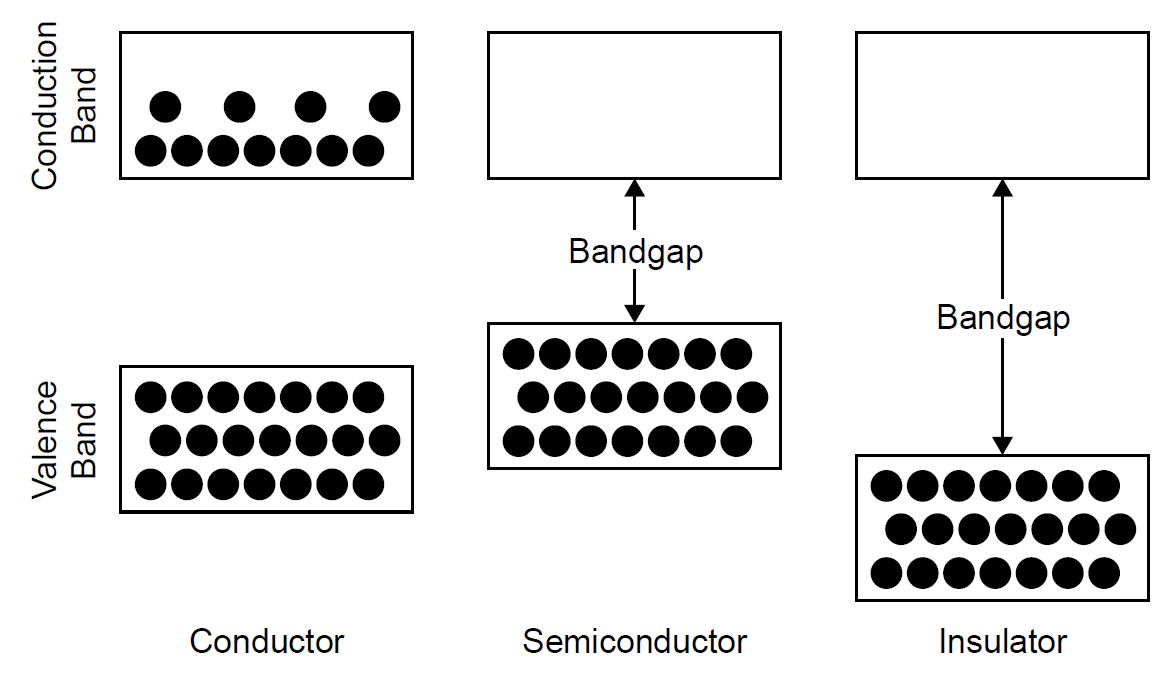
Figure 1.1. Electron energy levels in various materials.
and the material can carry current. The energy levels of electrons in each type of material are outlined in Figure 1.1. At its lowest energy state (i.e., with no energy applied and at a temperature of absolute zero) a semiconductor material has all electrons in the valence band, so there are no free electrons. In this state the material does not conduct electrical current (since there are no free electrons to do so) and thus acts like a perfect insulator. To conduct electric current, some electrons must be made to jump from the valence band to the conduction band, where, by definition, electrons are free to travel through the crystal (and hence current flows through the semiconductor). The energy that must be injected into the semiconductor to cause an electron to jump the gap between the valence band (where the electron is bound inside the atom) and the conduction band (where the electron is unbound) is called the band gap energy (denoted Eg). The band gap literally represents the energy difference between the levels of the two bands. When enough energy is absorbed by the atom (either by thermal excitation or perhaps by absorption of an incident photon), electrons may move to the next highest band, the conduction band. As temperature rises, then, we expect a semiconductor material to become more conductive of electric current. The minimum energy to cause this jump is equal to the band gap energy Eg, so in the case of a photon as the incident excitation source, the energy of the photon (hv) must be at least equal to Eg. When an electron jumps the gap from the valence band, it creates a vacancy or hole in the valence band of the atom (i.e., it is devoid of an electron normally there). A hole, as one might imagine, is a positive charge relatively speaking, since it is the absence of a negative charge that would normally be there to give a net charge of zero. The process results in the production of an electron hole pair, shown in Figure 1.2. The free electron, with energy in the conduction band, may wander through the crystal and eventually fill a hole in a valence band. In doing so, energy of the system must be conserved. This recombination process, called electron hole
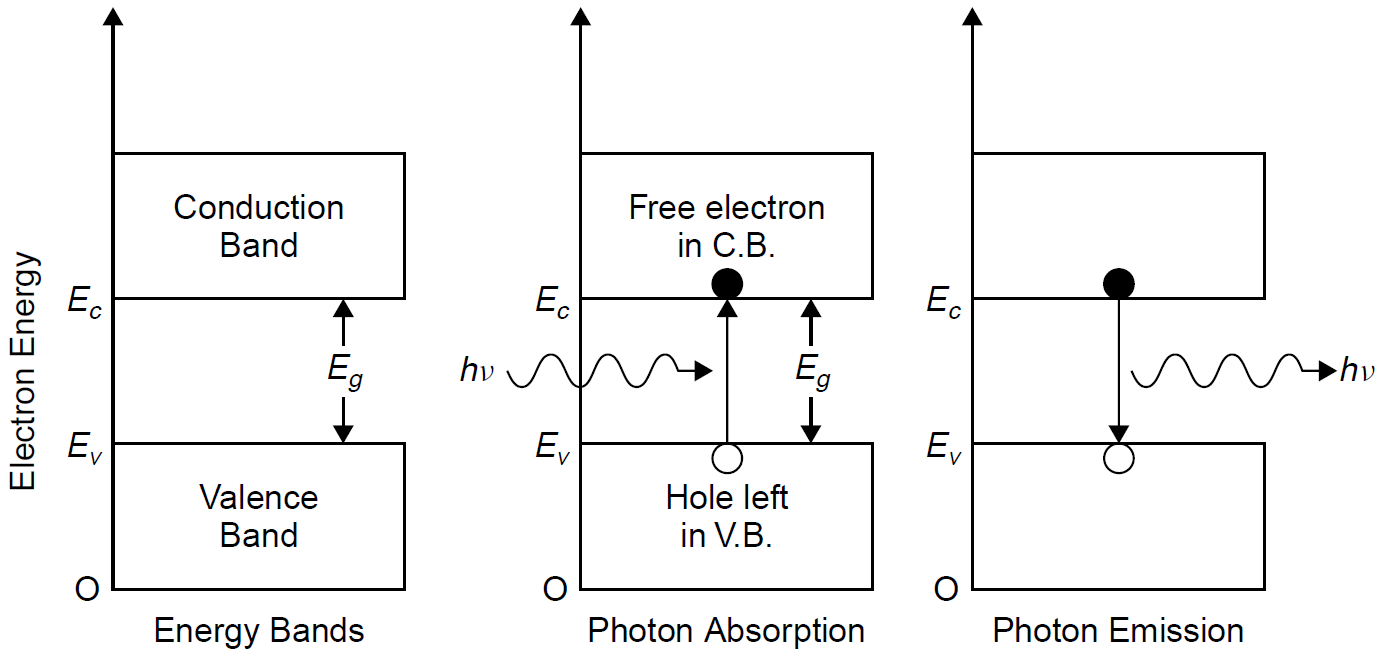
Figure 1.2. Absorption and emission in a semiconductor.
pair (EHP) recombination, results in either emission of a photon or production of heat in the crystal. The characteristics of the energy bands in a given semiconductor material may be modified by doping the material when it is grown. Silicon, in its purest form (called an intrinsic semiconductor), is not a good conductor of current. There are just enough electrons in the crystal to fill the valence band entirely, with none left for the conduction band, so it is almost unoccupied. For a given temperature, Boltzmann statistics can be used to predict the population of electrons in a given energy state (e.g., the conduction band), so even at an elevated temperature it will be found that few electrons are promoted to the conduction band. By adding impurities to the silicon (a process called doping) it can be made to have an excess of electrons which will then populate the conduction band. Adding dopants such as phosphorus or arsenic creates a type of silicon with excess electrons (in the conduction band) called n-type silicon. These dopants feature five valence electrons: Four bond with neighboring silicon atoms, leaving one “spare” electron. The spare electron is easily promoted to the conduction band (usually, by thermal energy), so the addition of an impurity such as this makes the silicon more conductive, since conductivity depends on the availability of charge carriers (in this case, electrons). This material will be unbalanced such that it will have more electrons than holes. In a similar way, the addition of other dopants, such as boron, make the silicon p-type, in which case it has a lack of electrons in the valence band and can accept extra electrons; in other words, extra holes are created in the valence band. This dopant has only three electrons, so bonds only to three neighboring silicon atoms, leaving one “hole” in the lattice (an un bonded electron in the silicon host material). Typical doping levels for either p- or n-type materials are small and usually on the order of 0.0001%. Electrons in the bands of each type of semiconductor are depicted in Figure 1.3. When n- and p-type semiconductors are brought into contact, a p-n junction (or diode) is formed. At the point of contact between the two materials, charge carriers (holes and electrons) diffuse across the junction and combine, forming a layer called the depletion layer, which is, literally, depleted of charge carriers, which combine
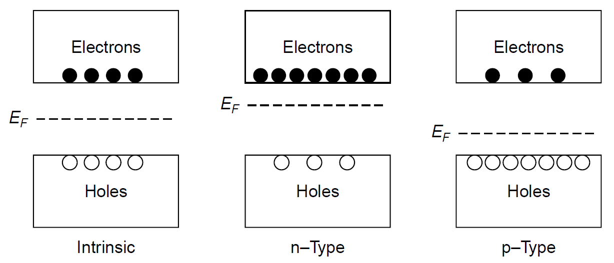
Figure 1.3. p- and n-type semiconductors.
rapidly the moment the junction is made. Excess negative charge forms in the p-region of the junction, and excess positive charge forms in the n-region of the junction, a barrier that effectively prevents more carriers from moving across the junction. In a p-n junction the Fermi levels (the energy value that has a 50% probability of being occupied by electrons, designated EF in Figure 1.3) align as required to form equilibrium at the contact point. In turn, the energies of the conduction and valence bands for each of the materials (p and n type) will be moved, with the levels of the n-type material falling. A contact potential develops between the two materials, a voltage that is required to be placed across the junction to make electrons jump the band gap and allow current to flow. This is the bias voltage of the diode and is about 0.7 V for a normal silicon diode to 1.7 V for a red gallium arsenide LED. When the diode is forward biased, meaning that a potential large enough to overcome the contact potential of the junction is applied, electrons are supplied to the n-type material and holes to the p-type material (i.e., current flow through the p-n junction). To maintain electrical equilibrium the excess injected carriers are removed by recombination of electron hole pairs in which electrons in the conduction band fall to the valence band, the result being the emission of a photon (in the case of an LED) or the production of heat by a non-radiative process (in most diodes used for signal applications). Figure 1.4 shows the flow of electrons and holes across the junction in a biased diode. LEDs can be designed to emit any color desired by changing the dopant concentration and hence the band gap voltage. Gallium arsenide can be doped to produce LEDs emitting red, orange, yellow, and green light. Blue and violet, on the other hand, require very large band gap energies, which are not possible using the same technology. An operating LED is shown in Figure 1.5. The diameter of the device is 5 mm; however, the device is mostly potting compound. The actual semiconductor 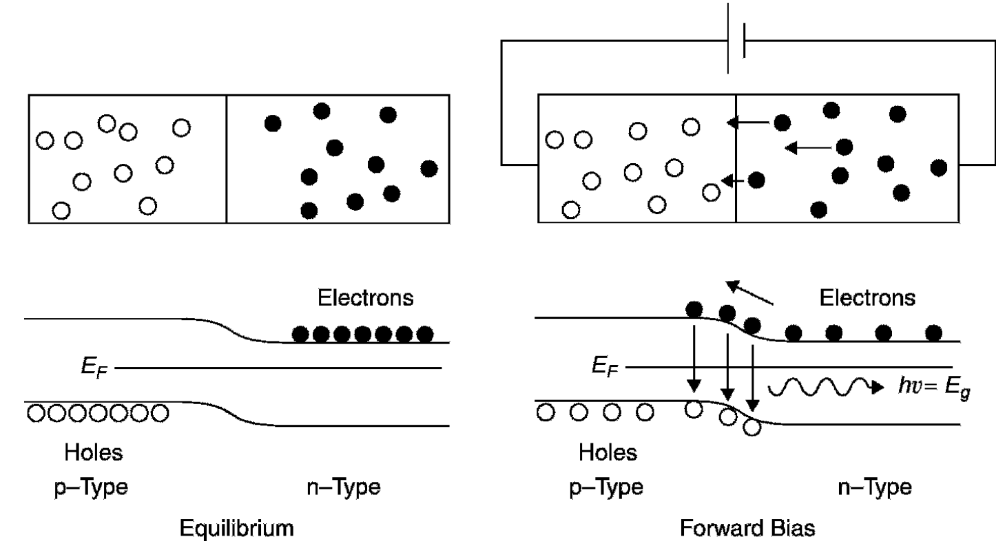
Figure 1.4. LED p-n junction at equilibrium and at forward bias.
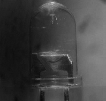
Figure 1.5. Light emitting diode.
crystal is the size of a grain of salt and is held within the cup-shaped terminal on the right. A thin wire connecting the terminal on the left to the crystal is visible in the photo. When operating, an LED requires a series resistance to limit current through the device since a diode connected directly to a voltage source (which exceeds the band gap voltage) will function as a dead short, drawing as much current as possible from the supply and failing rapidly. When high currents pass through the device, the metals comprising the p-n junction can literally melt, destroying the device. Most common LEDs glow brightly when a current between 10 and 20 mA is passed through them (although today, some high-brightness LEDs specify a maximum current in the hundreds of milli-amperes range). If a red LED with a bias voltage of 1.7 V is connected to a 5-V source, the series resistance may be calculated using Ohm’s law as follows:
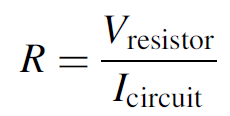 (1.1)
(1.1)
where R is the series resistance, Vresistor the voltage across the resistor, and Icircuit the series current in the circuit. Since this is a series circuit, the current through the resistor is the same as the current in the LED in this case, 10 mA. With a 5-V supply and 1.7 V across the LED, the expected voltage drop across the series resistor will be 3.3 V. Using formula (1.1), the required resistance is found to be 3.3 V/10 mA, or 330 Ω. The circuit is shown in Figure 1.6. When an LED of a different color is employed, both the bias voltage and the resistance value will change. A change in supply voltage will also necessitate a change in series resistance. It is important to note that all semiconductor diodes will not conduct until the forward bias voltage is reached. Figure 1.7 shows the experimentally determined

Figure 1.6. Use of a series resistance with an LED.
current voltage (I-V) curves for various diodes, including a silicon diode and two gallium arsenide (LED) diodes. No current (except perhaps a small leakage current under 1 μA caused by impurities in the materials) flows until the bias voltage is reached, after which the voltage across the device stays relatively constant and independent of current. In Figure 1.7, voltage (on the x-axis) is calibrated in units of 200 mV per division. Counting almost 3 divisions before the silicon diode conducts current, the forward bias of this diode is determined to be about 600 mV. Similarly, the red LED is found to have a bias voltage of 1.5 V and the yellow LED a bias voltage of 1.75 V. It is not surprising that the color of emission for an LED depends on the bias voltage: More energy (and hence a larger band gap) is required to produce shorter wavelengths of light (yellow) than longer wavelengths (red) since the photon energy corresponds to the band gap.
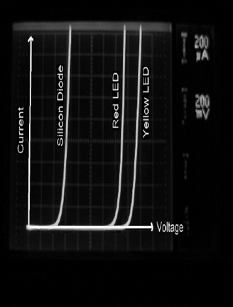
Figure 1.7. Current voltage curves for various diodes.
At this point it is necessary to differentiate between two types of semiconductors. As we shall see in the next section, the type of material affects whether or not light will be emitted during conduction. The first type, called indirect-gap semiconductors, have energy levels in each band such that an electron making a transition between the valence and conduction bands must experience a change of both energy and momentum. This is dictated by the principle of conservation of both energy and momentum, which occurs during any transition. In the case of a simple indirect gap diode conducting current, transitions from the valence to the conduction band occur only if energy (sufficient to jump the band gap) is supplied as well as momentum. The momentum is supplied by physical vibrations in the crystal lattice of the semiconductor material. When a downward transition occurs (from the conduction band to the valence band) the change of energy may result in production of a photon as expected; however, the change in momentum also results in production of a phonon a physical vibration in the crystal lattice. Most common semiconductors used for electronics purposes, such as silicon and germanium, are indirect gap semiconductors, and most do not emit photons as a result of recombination but rather, produce phonons, which are eventually manifested as heat in the material. In direct-gap semiconductors the momentum of an electron in either band is almost identical, so no real change in momentum occurs during a transition. Transitions of this type occur in one step, with energy conserved by the emission of a photon and no (or very little) change in momentum required. Gallium arsenide and similar materials used for LEDs and semiconductor lasers are direct-gap semiconductors. In the case of a gallium arsenide diode conducting current, a photon incident on the semiconductor can inject energy, absorbed by an electron in the material, without momentum. A single photon can result in a single electron making the jump across the band gap. In addition, the recombination of excess electrons and holes in such a device results in production of a photon with energy equal to the jump made across the band gap in theory the difference between the top of the valence and the bottom of the conduction bands. An applied forward bias voltage on a gallium arsenide p-n junction generates excess charge carriers near the depletion layer. Excess carriers recombine and photons are emitted.

|
|
|
|
مخاطر عدم علاج ارتفاع ضغط الدم
|
|
|
|
|
|
|
اختراق جديد في علاج سرطان البروستات العدواني
|
|
|
|
|
|
|
مدرسة دار العلم.. صرح علميّ متميز في كربلاء لنشر علوم أهل البيت (عليهم السلام)
|
|
|