
N-CHANNEL AND P-CHANNEL
 المؤلف:
S. Gibilisco
المؤلف:
S. Gibilisco
 المصدر:
Physics Demystified
المصدر:
Physics Demystified
 الجزء والصفحة:
412
الجزء والصفحة:
412
 22-10-2020
 2344
2344
N-CHANNEL AND P-CHANNEL
A simplified drawing of an n-channel JFET and its schematic symbol are shown in Fig. 1 a and b. The n-type material forms the path for the current. The majority carriers are electrons. The drain is positive with respect to the source. The gate consists of p-type material. Another, larger section of p-type material, the substrate, forms a boundary on the side of the channel opposite the gate. The voltage on the gate produces an electrical field that interferes with the flow of charge carriers through the channel. The more negative EG becomes, the more the electrical field chokes off the current though the channel, and the smaller ID gets.
A p-channel JFET (see Fig. 1c and d) has a channel of p-type semiconductor. The majority of charge carriers are holes. The drain is negative with respect to the source. The gate and substrate are n-type material. The more positive EG becomes, the more the electrical field chokes off the current through the channel, and the smaller ID gets. In engineering circuit diagrams, the n-channel JFET can be recognized by an arrow pointing inward at the gate and the p-channel JFET by an arrow pointing outward. The power-supply polarity also shows which type of device is used. A positive drain indicates an n-channel JFET, and a negative drain indicates a p-channel type.
An n-channel JFET almost always can be replaced with a p-channel JFET and the power-supply polarity reversed, and the circuit will still work if the new device has the correct specifications.
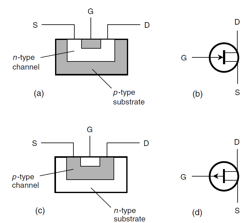
Fig. 1. Pictorial diagram of an n-channel JFET (a), schematic symbol for an n-channel JFET (b), pictorial diagram of a p-channel JFET (c), and schematic symbol for a p-channel JFET (d).
 الاكثر قراءة في أشباه الموصلات
 اخر الاخبار
اخبار العتبة العباسية المقدسة


