آخر المواضيع المضافة

 الفيزياء الكلاسيكية
الكهربائية والمغناطيسية
علم البصريات
الفيزياء الحديثة
النظرية النسبية
الفيزياء النووية
فيزياء الحالة الصلبة
الليزر
علم الفلك
المجموعة الشمسية
الطاقة البديلة
الفيزياء والعلوم الأخرى
مواضيع عامة في الفيزياء
الفيزياء الكلاسيكية
الكهربائية والمغناطيسية
علم البصريات
الفيزياء الحديثة
النظرية النسبية
الفيزياء النووية
فيزياء الحالة الصلبة
الليزر
علم الفلك
المجموعة الشمسية
الطاقة البديلة
الفيزياء والعلوم الأخرى
مواضيع عامة في الفيزياء| How the junction works |


|
|
Read More
Date: 7-4-2021
Date: 12-5-2021
Date: 5-4-2021
|
How the junction works
When the N-type material is negative with respect to the P-type, electrons flow easily from N to P. The N-type semiconductor, which already has an excess of electrons, gets even more; the P-type semiconductor, with a shortage of electrons, is made even more deficient. The N-type material constantly feeds electrons to the P-type in an attempt to create an electron balance, and the battery or power supply keeps robbing electrons from the P-type material. This is shown in Fig. 1A and is known as forward bias.
When the polarity is switched so the N-type material is positive with respect to the P type, things get interesting. This is called reverse bias. Electrons in the N-type material
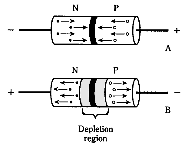
Fig. 1: At A, forward bias of a P-N junction; at B, reverse bias. Electrons are shown as small dots, and holes are shown as open circles.
are pulled towards the positive charge, away from the junction. In the P-type material, holes are pulled toward the negative charge, also away from the junction. The electrons (in the N-type material) and holes (in the P type) are the majority charge carriers. They become depleted in the vicinity of the P-N junction (Fig. 1B). A shortage of majority carriers means that the semiconductor material cannot conduct well. Thus, the depletion region acts like an insulator.


|
|
|
|
التوتر والسرطان.. علماء يحذرون من "صلة خطيرة"
|
|
|
|
|
|
|
مرآة السيارة: مدى دقة عكسها للصورة الصحيحة
|
|
|
|
|
|
|
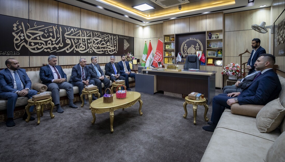
نحو شراكة وطنية متكاملة.. الأمين العام للعتبة الحسينية يبحث مع وكيل وزارة الخارجية آفاق التعاون المؤسسي
|
|
|