The k-Space Diagrams of Si and GaAs
Figure 1.1 shows an E versus k diagram of gallium arsenide and of silicon. These simpliflied diagrams show the basic properties considered in this text, but do not show many of the details more appropriate for advanced-level courses.
Note that in place of the usual positive and negative k axes, we now show two different crystal directions. The E versus k diagram for the one-dimensional model
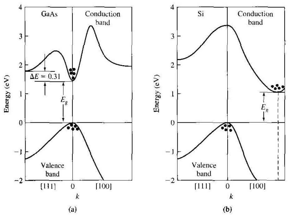
Figure 1.2 Energy band structures of (a) GaAs and (b) Si.
was symmetric ink so that no new information is obtained by displaying the negative axis. It is normal practice to plot the [100] direction along the normal +k axis and to plot the [111] portion of the diagram so the +k points to the left. In the case of diamond or zincblende lattices, the maxima in the valence band energy and minima in the conduction band energy occur at k = 0 or along one of these two direction.
Figure 1.2a shows the E versus k diagram for GaAs. The valence band maximum and the conduction hand minimum both occur at k = 0. The electrons in the conduction band tend to settle at the minimum conduction band energy which is at k = 0. Similarly, holes in the valence band tend to congregate at the uppermost valence band energy. In GaAs, the minimum conduction band energy and maximum valence band energy occur at the same k value. A semiconductor with this property is said to be a direct bandgap semiconductor; transitions between the two allowed bands can take place with no change in crystal momentum. This direct nature has significant effect on the optical properties of the material. GaAs and other direct bandgap materials are ideally suited for use in semiconductor lasers and other optical devices.
The E versus k diagram for silicon is shown in Figure 1.2b. The maximum in the valence band energy occurs at k = 0 as before. The minimum in the conduction hand energy occurs not at k = 0, hut along the [100] direction. The difference between the minimum conduction band energy and the maximum valence band energy is still defined as the bandgap energy Eg. A semiconductor whose maximum valence band energy and minimum conduction band energy do not occur at the same k value is called an indirect bandgap semiconductor. When electrons make a transition between the conduction and valence bands, we must invoke the law of conservation of momentum. A transition in an indirect bandgap material must necessarily include an interaction with the crystal so that crystal momentum is conserved.
Germanium is also an indirect bandgap material, whose valence band maximum occurs at k = 0 and whose conduction band minimum occurs along the [111] direction. GaAs is a direct bandgap semiconductor, but other compound semiconductor, such as Gap and AlAs, have indirect bandgaps.


