تاريخ الفيزياء
علماء الفيزياء


الفيزياء الكلاسيكية
الميكانيك
الديناميكا الحرارية
الكهربائية والمغناطيسية
الكهربائية
المغناطيسية
الكهرومغناطيسية
علم البصريات
تاريخ علم البصريات
الضوء
مواضيع عامة في علم البصريات
الصوت
الفيزياء الحديثة
النظرية النسبية
النظرية النسبية الخاصة
النظرية النسبية العامة
مواضيع عامة في النظرية النسبية
ميكانيكا الكم
الفيزياء الذرية
الفيزياء الجزيئية
الفيزياء النووية
مواضيع عامة في الفيزياء النووية
النشاط الاشعاعي
فيزياء الحالة الصلبة
الموصلات
أشباه الموصلات
العوازل
مواضيع عامة في الفيزياء الصلبة
فيزياء الجوامد
الليزر
أنواع الليزر
بعض تطبيقات الليزر
مواضيع عامة في الليزر
علم الفلك
تاريخ وعلماء علم الفلك
الثقوب السوداء
المجموعة الشمسية
الشمس
كوكب عطارد
كوكب الزهرة
كوكب الأرض
كوكب المريخ
كوكب المشتري
كوكب زحل
كوكب أورانوس
كوكب نبتون
كوكب بلوتو
القمر
كواكب ومواضيع اخرى
مواضيع عامة في علم الفلك
النجوم
البلازما
الألكترونيات
خواص المادة
الطاقة البديلة
الطاقة الشمسية
مواضيع عامة في الطاقة البديلة
المد والجزر
فيزياء الجسيمات
الفيزياء والعلوم الأخرى
الفيزياء الكيميائية
الفيزياء الرياضية
الفيزياء الحيوية
الفيزياء والفلسفة
الفيزياء العامة
مواضيع عامة في الفيزياء
تجارب فيزيائية
مصطلحات وتعاريف فيزيائية
وحدات القياس الفيزيائية
طرائف الفيزياء
مواضيع اخرى

The Energy Band and the Bond Model
 المؤلف:
Donald A. Neamen
المؤلف:
Donald A. Neamen
 المصدر:
Semiconductor Physics and Devices
المصدر:
Semiconductor Physics and Devices
 الجزء والصفحة:
p 70
الجزء والصفحة:
p 70
 14-5-2017
 923
923


+
-
20
The Energy Band and the Bond Model
We discussed the covalent bonding of silicon. Figure 1.1 shows a two dimensional representation of the covalent bonding in a single-crystal silicon lattice. This figure represents silicon at T = 0 Kin which each silicon atom is surrounded by eight valence electrons that are in their lowest energy state and are directly involved in the covalent bonding. At T = 0 K, the 4N states in the lower band, the valence band, are filled with the valence electrons. All of the valence electrons schematically shown in Figure 1.1 are in the valence band. The upper energy band, the conduction band, is completely empty at T = 0 K.
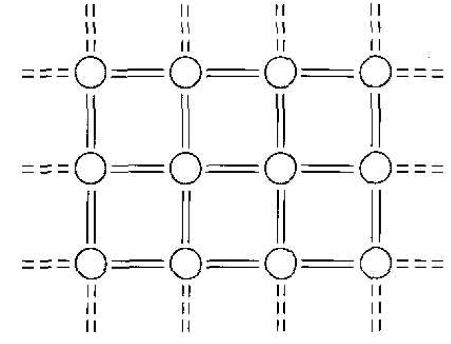
Figure 1.1 Two-dimensional representation of the covalent bonding in a semiconductor at T = 0 K.
As the temperature increases above 0 K, a few valence band electrons may gain enough thermal energy to break the covalent bond and jump into the conduction band. Figure 1.2a shows a two-dimensional representation of this bond-breaking effect and Figure 1.2b. a simple line representation of the energy-band model, shows the same effect.
The semiconductor is neutrally charged. This means that, as the negatively charged electron breaks away from its covalent bonding position, a positively charged "empty state" is created in the original covalent bonding position in the valence band. As the temperature further increases, more covalent bonds are broken, more electrons jump to the conduction hand, and more positive "empty states" are created in the valence band.
We can also relate this bond breaking to the E versus k energy bands. Figure 1.3a shows the E versus k diagram of the conduction and valence bands at

Figure 1.2 (a) Two-dimensional representation of the breaking of a covalent bond. (b) Corresponding line representation of the energy band and the generation of a negative and positive charge with the breaking of a covalent bond.
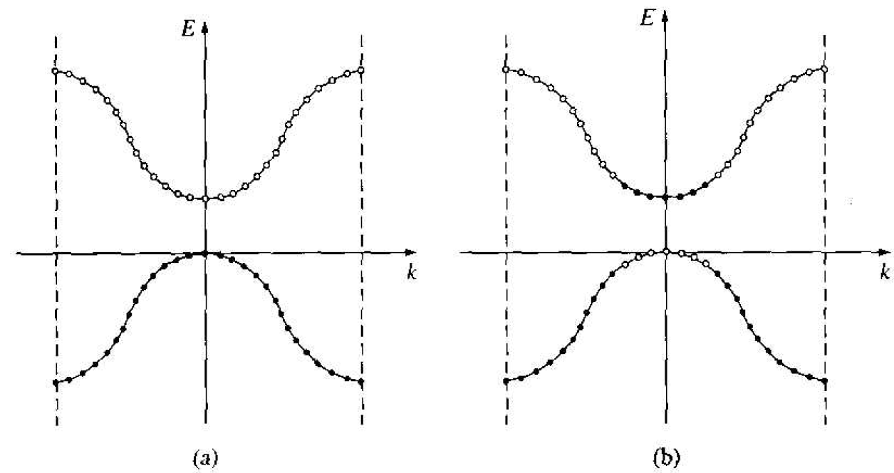
Figure 1.3 The E versus k diagram of the conduction and valence bands of a semiconductor at (a) T = 0 K and (b) T > 0 K.
T = 0 K. The energy states in the valence band are completely full and the states in the conduction band are empty. Figure 1.3b shows these same bands for T > 0 K, in which some electrons have gained enough energy to jump to the conduction band and have left empty states in the valence band. We are assuming at this point that no external forces are applied so the electron and "empty state" distributions are symmetrical with k.
 الاكثر قراءة في الموصلات
 اخر الاخبار
اخبار العتبة العباسية المقدسة

الآخبار الصحية


 قسم الشؤون الفكرية يصدر كتاباً يوثق تاريخ السدانة في العتبة العباسية المقدسة
 "المهمة".. إصدار قصصي يوثّق القصص الفائزة في مسابقة فتوى الدفاع المقدسة للقصة القصيرة
 (نوافذ).. إصدار أدبي يوثق القصص الفائزة في مسابقة الإمام العسكري (عليه السلام)