One-dimensonal control: carbon nanotubes and inorganic nanowires
Key point: Dimensionality plays a crucial role in determining the properties of materials. The elongated one-dimensional morphology of nanorods, nanowires, nanofibres, nanowhiskers, nanobelts, and nanotubes has been studied extensively because one-dimensional systems are the lowest dimensional structures that can be used for efficient transport of electrons and optical excitation. They are therefore expected to be crucial to the function and integration of nanoscale devices. Not much is known, however, about the nature of localization that could preclude transport through one-dimensional systems. Such systems should possess discrete molecular-like states extending over large distances and exhibit some exotic phenomena, such as the effective separation of the spin and charge of an electron. There are also many applications where one-dimensional nanostructures could be exploited, including nanoelectronics, very strong and tough composites, functional nanostructured materials, and novel probe microscopy tips. To address these fascinating fundamental scientific issues and potential applications, two important questions pose key challenges to the fields of condensed matter chemistry and physics research. First, how can atoms or other building blocks be assembled rationally into structures with nanometre-sized diameters but much greater lengths? Second, what are the intrinsic properties of these quantum wires and how do these properties depend, for example, on their diameter and their structure? A key class of nanomaterials that offers potential answers to these questions is carbon nanotubes (CNTs). Carbon nanotubes are perhaps the best example of novel nanostructures fabricated through bottom-up chemical synthesis approaches. They have very simple chemical composition and atomic bonding configuration but exhibit remarkably diverse structures and unparalleled physical properties. These novel materials have found application as chemical sensors, fuel cells, field effect transistors, electrical interconnects, and mechanical reinforcers. The structure and properties of buckminsterfullerene, C60, and related species have produced much activity in the chemistry and materials sciences communities. The now familiar soccer-ball structure of C60 itself was discussed in Chapter 14. Carbon nanotubes were discovered in the early 1990s by electron microscopy. The bonding, local coordination, and general structure of CNTs are similar to those of buckminsterfullerene, but CNTs can have a greatly extended length, leading to a tube rather than a ball structure (Fig. 25.16).
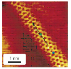
Figure 25.16 STM image of a single-walled carbon nanotube. (J. Hu, et al., Acc. Chem. Res., 1999, 32, 435.) (Reproduced with permission from the American Chemical Society.)
Carbon nanotubes are cylindrical shells formed conceptually by rolling graphene (graphitelike) sheets into closed tubular nanostructures with diameters matching that of C60 (0.5 nm) but lengths up to micrometres. A single-walled nanotube (SWNT) is formed by rolling a sheet of graphene into a cylinder along an (m,n) lattice vector in the graphene plane (Fig. 25.17). The (m,n) indices determine the diameter and chirality of the CNT, which in turn control its physical properties. Most CNTs have closed ends where hemispherical units cap the hollow tubes.
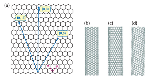
Figure 25.17 (a) The honeycomb structure of a graphene sheet. Single-walled carbon nanotubes can be formed by folding the sheet along lattice vectors, two of which are shown as a1 and a2. Folding along the (8,8), (8,0), and (10,–2) vectors leads to armchair (b), zigzag (c), and chiral (d) tubes, respectively. (Based on H. Dai, Acc. Chem. Res., 2002, 35, 1035.) (Reproduced with permission from the American Chemical Society.)
Carbon nanotubes self-assemble into two distinct classes, SWNTs and multiwalled carbon nanotubes (MWNTs). In MWNTs, the tube wall is composed of multiple graphene sheets. Morphosynthetic control provides routes to tune the details of these self-assembled nanostructures. This self-assembly occurs during synthesis using several of the fabrication techniques we have already described, including pulsed laser ablation, laser-assisted catalytic growth, chemical vapour deposition (CVD) based on hydrocarbon gases, and carbon arc discharge. All these strategies rely on vaporizing carbon and condensing some fraction into extended nanostructures. Laser vaporization methods typically make relatively small amounts of nanocarbons; specialized CVD techniques have been developed to synthesize CNTs in quantities in excess of a few milligrams. In the CVD approach, a hydrocarbon gas such as methane is decomposed at elevated temperatures and C atoms are condensed on to a cooled substrate that may contain various catalysts, such as Fe. This CVD method is attractive because it produces open-ended tubes (which are not produced in the other methods), allows continuous fabrication, and can easily be scaled up to large-scale production. Because the tubes are open, the method also allows for the use of the nanotube as a templating agent. In the arc discharge method, extremely high temperatures are obtained by shorting two carbon rods together, which causes a plasma discharge. Such plasmas easily achieve temperatures in excess of where carbon vaporizes (at about 4500 K). Low potential differences and moderately high currents are needed to produce this arc. The typical CNT formed by either the arc method or CVD is multiwalled. To encourage SWNT formation, it is necessary to add a metal catalyst such as Co, Fe, or Ni to the carbon source. These metal catalyst particles block the end-cap of each carbon hemisphere and thus promote SWNT growth. In addition, the growth directions of the nanotubes can be controlled by van der Waals forces, applied electric fields, and patterning of the metal catalyst onto different substrates. The patterned growth approach is feasible with discrete catalytic nanoparticles and scalable on large wafers to achieve large arrays of nanowires (Fig. 25.18).
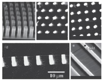
Figure 25.18 Ordered carbon nanotube structures obtained by direct chemical vapour deposition synthesis. (a) An SEM image of self-oriented MWNT arrays. Each tower-like structure is formed by many closely packed multiwalled nanotubes. Nanotubes in each tower are oriented perpendicular to the substrate. (b) SEM top view of a hexagonal network of SWNTs (the line-like structures) suspended on top of silicon posts (the bright dots). (c) SEM top view of a square network of suspended SWNTs. (d) Side view of a suspended SWNT power line on silicon posts (the bright lines). (e) SWNTs suspended by silicon structures (the bright regions). The nanotubes are aligned along the electric field direction. (H. Dai, Acc. Chem. Res., 2002, 35, 1035.) (Reproduced with permission from the American Chemical Society.) The repeating axial hexagonal patterns of CNTs are graphitic structures; however, the electrical properties of nanotubes depend on the relative orientation of the repeating hexagons. The nanotubes can be either semiconductors or metallic conductors. When oriented in the chair configuration, CNTs exhibit remarkably high electrical conductivity. Electrons can travel through the micrometre-length nanowire with zero scattering and zero heat dissipation. CNTs also have very high thermal conductivity, comparable to the best thermal conductors known (such as their counterparts, diamond and graphite). Therefore, they are being heralded as the ideal nanomaterial for the development of interconnects for integrated circuits. They may solve two key challenges in the computer industry: heat dissipation and increased processing speeds. Open-ended CNTs can also be used for nanorobotic spot welding to deposit metal at specific sites for connections in integrated circuits (Fig. 25.19). Copper is a good choice for these applications because it has high thermal and electrical conductivity. It also has a very low bonding energy to C (0.10–0.14 eV/atom), so can be deposited easily on surfaces and structures from the encapsulating CNT. The deposition is accomplished by making physical contact between a STM probe and a copper-filled CNT tip, and then applying a potential difference to create a circuit with the probe as the anode. This procedure generates sufficient heat for the Cu atoms to be able to migrate along the tube and be deposited where they are required. The nanowelding process is of interest because its advantages include efficiency (a very low current can induce melting and flow), three-dimensional manipulation of welding site by using piezoelectric distortion, rapid melting, precise control of small mass delivery, and the compatibility of Cu with conventional semiconductors. In addition to CNTs, parallel methods have been discovered for making nanotubes out of materials that share bonding characteristics with C, including semiconductors and metal oxides. More specifically, BN, ZnO, ZnSe, ZnS, InP, GaAs, InAs, and GaN have all been made into nanotubes. The novel electronic properties and small sizes of these nanotubes make them appealing as inorganic nanowires. Core–sheath wires similar to macroscopic coaxial wires are of great interest. One method to prepare them uses a colloid-templating strategy that involves a layer-by-layer assembly of polyelectrolytes and inorganic nanoparticles on submicrometre- and micrometre-sized polystyrene (PS) latex particles. A number of methods, including laser ablation, carbothermal reduction, and several solution-based methods, have been developed to generate one-dimensional nanostructures with coaxial structures. For instance, by using a novel nanowire-templating technique based on the layer-by-layer approach and calcining (heating in air to drive off volatile templating agents), ordered Au/TiO2 core–sheath nanowire arrays have been fabricated. A template-grown gold nanowire array is used as a positive template, and then a cationic polyelectrolyte and an inorganic precursor are assembled on gold nanowires by the layer-by-layer technique. Calcination then converts the inorganic precursor to titanium dioxide (Fig. 25.20).
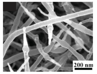
Figure 25.19 FESEM image of Cu-filled CNTs; all have sharp tips filled with metal nanoneedles. These CNTs are up to 5 µm long, with outer diameters in a range of 40–80 nm. (L. X. Dong, et al., Nano Lett. 2007, 7, 58.)
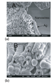
Figure 25.20 (a) Low-magnification and (b) high-magnification SEM images of Au/TiO2 core–sheath nanowire arrays. (Y.-G. Guo, et al., J. Phys. Chem. B, 2003, 107, 5441.) An advantage of the layer-by-layer nanowire-templating approach over other methods is that nanoscale control can be exerted over the sheath thickness by varying the number of deposition cycles. Titanium dioxide has been one of the most investigated oxide materials because of its technological importance. It has been widely used for photocatalysis and environmental clean-up applications, on account of its strong oxidizing power, chemical inertness, and nontoxicity. These core–sheath nanowires have well-defined diameters and lengths, largely determined by the dimensions of the templates, and porous sheaths with thicknesses controlled by the number of layers deposited. This method opens a door to the use of a wide variety of nanowires as the positive templates for the fabrication of core–sheath nanostructured materials for chemical sensors, photocatalysis, light energy conversion devices, and nanoscale electronic and optoelectronic devices. More specifically, Au and Ag nanowires have been targeted as scaffolds for optical sensing of environmentally and biologically important analytes with very high selectivity and sensitivity.


